SAM
Motorola MC6883 Synchronous Address Multiplexer known as the SAM
COLOR COMPUTER 1 AND 2
Color Computers 1 and 2 shipped with 4, 16, 32, or 64KB of RAM depending on options and board.
The Color Computers 1 and 2 were equipped with a Synchronous Address Multiplexer (SAM MC6883) to manage memory configuration and refresh for the MPU and VDG.

~ Color Computer Technical Reference Manual, 1981, page 8
COLOR COMPUTER 3
Color Computer 3 shipped with 128 or 512KB of RAM depending on options chosen.
The Color Computer 3 custom GIME chip included emulation for the previous generation's SAM chip as well as provided a new Memory Management Unit MMU for working with memory larger than 64KB.
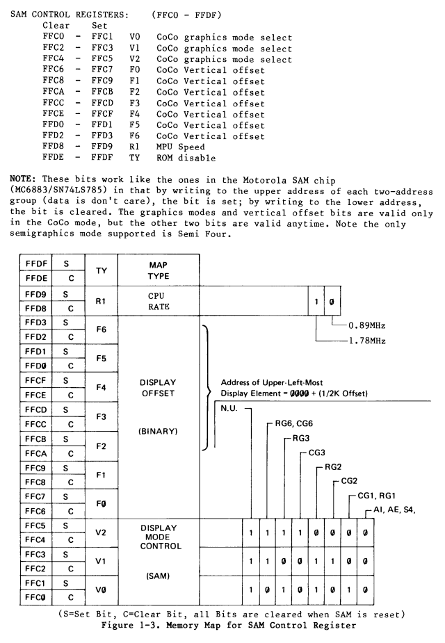
SAM CONTROL REGISTER
The SAM CONTROL REGISTER has 16 “inputs”
VDG ADDRESSING MODES "V" BITS
These bits work in conjunction with the G/A, GM2-GM0, and CSS bits in the VDG to set the video mode on CoCo 1 and 2.
| OFF | ON | PURPOSE |
|---|---|---|
| FFC0 | FFC1 | VDG Address Mode bit V0 |
| FFC2 | FFC3 | VDG Address Mode bit V1 |
| FFC4 | FFC5 | VDG Address Mode bit V2 |
| V2 | V1 | V0 | ADDRESS MODE |
|---|---|---|---|
| 0 | 0 | 0 | AI Alphanumeric Internal |
| 0 | 0 | 0 | AE Alphanumeric External |
| 0 | 0 | 0 | S4 Semigraphics 4 |
| 0 | 0 | 0 | S6 Semigraphics 6 |
| 0 | 0 | 1 | G1C Graphics 1 Color |
| 0 | 0 | 1 | G1R Graphics 1 Resolution |
| 0 | 1 | 0 | S8 Semigraphics 8 (only partially supported on CoCo 3) |
| 0 | 1 | 0 | G2C Graphics 2 Color |
| 0 | 1 | 1 | G2R Graphics 2 Resolution (PMODE0) |
| 1 | 0 | 0 | S12 Semigraphics 12 (only partially supported on CoCo 3) |
| 1 | 0 | 0 | G3C Graphics 3 Color (PMODE1) |
| 1 | 0 | 1 | G3R Graphics 3 Resolution (PMODE 2) |
| 1 | 1 | 0 | S24 Semigraphics 24 (only partially supported on CoCo 3) |
| 1 | 1 | 0 | G6C Graphics 6 Color (PMODE3) |
| 1 | 1 | 0 | G6R Graphics 6 Resolution (PMODE4) |
| 1 | 1 | 1 | G6R Graphics 6 Resolution DMA |
VDG ADDRESS OFFSET "F" BITS
Base page address equals 512 * binary value of Offset bits F6-F0
| OFF | ON | PURPOSE |
|---|---|---|
| FFC6 | FFC7 | Offset bit F0 |
| FFC8 | FFC9 | Offset bit F1 |
| FFCA | FFCB | Offset bit F2 |
| FFCC | FFCD | Offset bit F3 |
| FFCE | FFCF | Offset bit F4 |
| FFD0 | FFD1 | Offset bit F5 |
| FFD2 | FFD3 | Offset bit F6 |
32 PAGE SWITCH "P" BIT
One bit (P1) is used “in place of” A15 from the MC6809E in order to refer access within $0000-$7FFF to one of two 32K byte pages of RAM.
If the system does not use more than 32K bytes of RAM, P1 can be ignored.
When using 4K x 1 RAMs, two banks of eight IC's are allowed.
This accounts for addresses $0000-$1FFF.
Also, this same RAM can be addressed at $2000-$3FFF, $4000-$5FFF, and $6000-$7FFF.
| OFF | ON | PURPOSE |
|---|---|---|
| FFD4 | FFD5 | 32k Page switch bit P |
| P | 32K PAGE SWITCH |
|---|---|
| 0 | MPU Addresses from $0000 to $7FFF apply to 32K Page #0 |
| 1 | MPU Addresses from $0000 to $7FFF apply to 32K Page #1 |
MPU RATE "R" BITS
| OFF | ON | PURPOSE |
|---|---|---|
| FFD6 | FFD7 | MPU Rate bit R0 |
| FFD8 | FFD9 | MPU Rate bit R1 |
| R1 | R0 | MPU RATE MHZ | ROM SPEED | RAM SPEED | RATE NAME |
|---|---|---|---|---|---|
| 1 | 1 | Unknown | Unknown | Unknown | Unknown |
| 1 | 0 | 1.8MHz | Fast | Fast | Fast E and Q clock is Freq / 8 |
| 0 | 1 | 0.9/1.8MHz | Fast | Slow | Address Dependent (AD) ROM E and Q is Freq / 8, RAM E and Q is Freq / 16 |
| 0 | 0 | 0.9 | Slow | Slow | Slow E and Q clock is Freq / 16 |
!!! MPU RATE R0 bit is not available on the CoCo 3 - only R1 is used !!!
MEMORY SIZE (RAM) "M" BITS
| OFF | ON | PURPOSE |
|---|---|---|
| FFDA | FFDB | Memory Size Bit 0 |
| FFDC | FFDD | Memory Size Bit 1 |
| M1 | M0 | MEMORY SIZE (RAM) |
|---|---|---|
| 1 | 1 | 64K static memory configuration (up to 64K SRAM with address latch) |
| 1 | 0 | 64K dynamic memory configuration (1 bank of 64K x 1 DRAM) |
| 0 | 1 | 16K dynamic memory configuration (1 or 2 banks of 16K x 1 DRAM) |
| 0 | 0 | 4K dynamic memory configuration (1 or 2 banks 4K x 1 DRAM) |
MEMORY MAP TYPE "TY" BIT
| OFF | ON | PURPOSE |
|---|---|---|
| FFDE | FFDF | Memory Map Type (TY) |
| TY | MEMORY MAP TYPE |
|---|---|
| 0 | Normal - ROM Selected - Slow, Address Dependent, or Fast MPU Rate may be used |
| 1 | ROM Deselected - only Slow MPU Rate may be used |
ASSEMBLY INCLUDE
The following EQUates define names for SAM registers which follow this naming scheme:
- Prefix: SAM
- Action: C for Clear, S for Set
- Bit Name: The name of the SAM Control Register bit that is set or cleared by strobing that address.
For example, strobing $FFC0 clears SAM VDG bit V0, so the register name is SAMCV0 “SAM Clear V0”
******************************************************************************
*** SYNCHRONOUS ADDRESS MULTIPLEXER (SAM) MC6883
******************************************************************************

                        ******************************************************
                        * COCO 1, 2 AND 3
SAMCV0  EQU     $FFC0   * SAM CLR VDG V0  000=AI,AE,S4,S6  100=G3C
SAMSV0  EQU     $FFC1   * SAM SET VDG V0  001=G1C,G1R      101=G3R
SAMCV1  EQU     $FFC2   * SAM CLR VDG V1  010=G2C          110=G6R,G6C
SAMSV1  EQU     $FFC3   * SAM SET VDG V1  011=G2R          111=DMA
SAMCV2  EQU     $FFC4   * SAM CLR VDG V2
SAMSV2  EQU     $FFC5   * SAM SET VDG V2

                        ******************************************************
                        * COCO 1, 2 AND 3
SAMCF0  EQU     $FFC6   * SAM CLR VDG F0  OFFSET=$0000 + ( 512 * F6-F0)
SAMSF0  EQU     $FFC7   * SAM SET VDG F0
SAMCF1  EQU     $FFC8   * SAM CLR VDG F1
SAMSF1  EQU     $FFC9   * SAM SET VDG F1
SAMCF2  EQU     $FFCA   * SAM CLR VDG F2
SAMSF2  EQU     $FFCB   * SAM SET VDG F2
SAMCF3  EQU     $FFCC   * SAM CLR VDG F3
SAMSF3  EQU     $FFCD   * SAM SET VDG F3
SAMCF4  EQU     $FFCE   * SAM CLR VDG F4
SAMSF4  EQU     $FFCF   * SAM SET VDG F4
SAMCF5  EQU     $FFD0   * SAM CLR VDG F5
SAMSF5  EQU     $FFD1   * SAM SET VDG F5
SAMCF6  EQU     $FFD2   * SAM CLR VDG F6
SAMSF6  EQU     $FFD3   * SAM SET VDG F6

                        ******************************************************
                        * !!! COCO 1 AND 2 ONLY !!!
SAMCP1  EQU     $FFD4   * SAM CLR PAGE P1  00=NORMAL
SAMSP1  EQU     $FFD5   * SAM SET PAGE P1  01=MPU $0000-$7FFF ON PAGE 1

                        ******************************************************
                        * !!! COCO 1 AND 2 ONLY !!!
SAMCR0  EQU     $FFD6   * SAM CLR MPU RATE R0  00=SLOW TRANSPARENT REFRESH
SAMSR0  EQU     $FFD7   * SAM SET MPU RATE R0  01=ADDRESS DEPENDENT

                        ******************************************************
                        * COCO 1, 2 AND 3
SAMCR1  EQU     $FFD8   * SAM CLR MPU RATE R1  10=FAST
SAMSR1  EQU     $FFD9   * SAM SET MPU RATE R1  11=FAST NO REFRESH

                        ******************************************************
                        * !!! COCO 1 AND 2 ONLY !!!
SAMCM0  EQU     $FFDA   * SAM CLR MEMORY SIZE M0 00=4K
SAMSM0  EQU     $FFDB   * SAM SET MEMORY SIZE M0 01=16K
SAMCM1  EQU     $FFDC   * SAM CLR MEMORY SIZE M1 10=64K DRAM
SAMSM1  EQU     $FFDD   * SAM SET MEMORY SIZE M1 11=64K SRAM

                        ******************************************************
                        * COCO 1, 2 AND 3
SAMCTY  EQU     $FFDE   * SAM CLR MAP TYPE 00=NORMAL ROM MODE
SAMSTY  EQU     $FFDF   * SAM SET MAP TYPE 01=RAM MODE

******************************************************************************
*** END OF SYNCHRONOUS ADDRESS MULTIPLEXER (SAM) MC6883
******************************************************************************
Many thanks to William “lostwizard” Astle for comments and corrections!
RTS
Return to Tandy Color Computer