VDG AND VDGT1
torstencito asked the following on the Color Computer Discord:
Regarding the T1 VDG: I know this is not pin compatible. Is there any short explanation why and what the differences are and if it would be possible to build an adapter to use a T1 in a classic VDG socket?
I am no VDG or hardware expert but I will take an initial crack since its an interesting question.
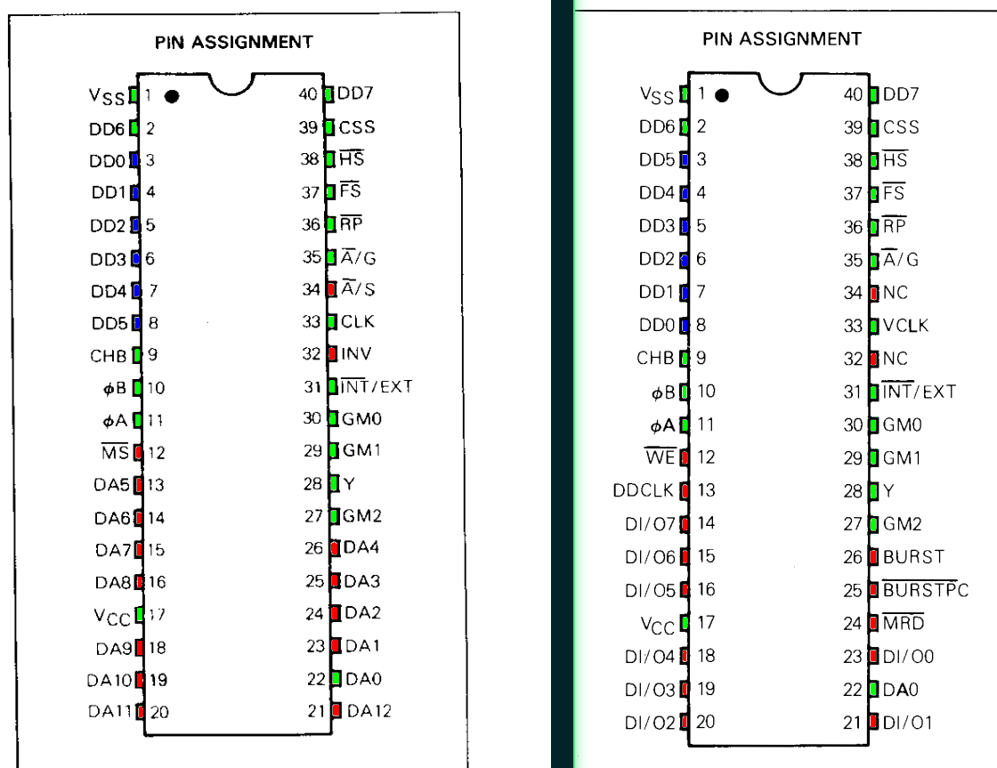
The picture is the VDG pinout on the left, and the T1 VDG on the right.
The pins in green are the same signals / functions … on the same pins … of both chips.
The pins in red are where pins handle different signals / functions chip versus chip.
The pins in blue are where the pins have the same basic signal / function, but have moved around between the chips.
Going pin by pin, signal by signal between the two chips there are three high-level differences that show up:
The T1 VDG pulls in the functionality and circuitry of an LS244 logic chip from the earlier CoCo motherboards.
This means that chip would have to be removed and bodge/jumper wires run to the interface board to use the T1's version of those signals.
The second difference is the change from DA1-DA12 to DI/O0 to DI/O7 … this is a fundamental change in how the VDGs access and use the memory system buses as the VDG or T1 reads system memory (sharing with the MPU and coordinated by the SAM)… and that “lockstep dance” of memory access is very motherboard specific.
A third difference is in how the “artifact colors” circuits work (tied to the /BURSTPC and BURST lines)
So, to summarize:
They are designed for different memory sizes and access and handle artifact colors different.. which are different motherboard and VDG chip designs - not just a VDG change alone.
So … now … hopefully someone who really knows can fix what I got wrong and make it simpler.
▲ Return to Top
